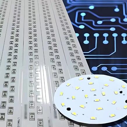
The Manufacturing Process of LED PCBs: From Design to Production
2024-09-04
The LED PCB (Printed Circuit Board) is a critical component in modern lighting solutions, ensuring that LEDs function efficiently and reliably. But how exactly are these PCBs made? Understanding the manufacturing process of LED PCBs provides insight into the precision and engineering required to produce high-quality LED lighting products. In this blog, we’ll walk through the stages of LED PCB manufacturing, from design to production.
Stage 1: Designing the LED PCB
1. Schematic Design
The first step in manufacturing an LED PCB is designing the schematic. This is a blueprint that outlines the electrical connections and layout of components on the PCB. Engineers use specialized software to create this design, ensuring that the LED array, resistors, capacitors, and other components are correctly placed and connected.
2. PCB Layout Design
Once the schematic is finalized, the PCB layout is created. This layout determines the physical placement of the components on the board and the routing of the conductive traces. The layout must consider factors such as heat dissipation, signal integrity, and mechanical stability.
3. Thermal Management Considerations
In LED PCB design, thermal management is a critical concern. The layout must include features that enhance heat dissipation, such as thermal vias, heat sinks, or the use of high-conductivity materials like aluminum or ceramic substrates.
4. Design Validation and Simulation
Before moving to production, the design is validated through simulation tools. These tools help identify potential issues, such as thermal hotspots, electrical interference, or mechanical stress points. Any necessary adjustments are made to the design before proceeding to the next stage.
Stage 2: Material Selection
1. Substrate Material
The choice of substrate material is crucial for the performance of the LED PCB. Common materials include:
- Aluminum: Known for its excellent thermal conductivity, aluminum is the most popular choice for high-power LED PCBs.
- FR-4: A fiberglass-reinforced epoxy laminate, FR-4 is used for lower-power applications where thermal management is less critical.
- Ceramic: Used in high-density applications requiring superior thermal performance and electrical insulation.
2. Copper Cladding
The next step is selecting the copper cladding, which forms the conductive traces on the PCB. The thickness of the copper layer is chosen based on the current-carrying requirements of the LED circuit.
3. Solder Mask and Silkscreen
The solder mask is applied to protect the copper traces from oxidation and prevent solder bridges between components during assembly. The silkscreen is used to print component labels, logos, and other information on the PCB.
Stage 3: PCB Fabrication
1. Etching
The first step in fabricating the PCB is etching the copper-clad substrate. This process involves applying a photoresist to the substrate, exposing it to UV light through a photomask, and then developing the resist to create the desired pattern. The exposed copper is then etched away, leaving only the desired conductive traces.
2. Drilling and Plating
After etching, holes are drilled into the PCB for component leads and vias. These holes are then plated with copper to create electrical connections between the layers of the PCB.
3. Laminating and Layering
For multi-layer PCBs, additional layers of substrate and copper are laminated together. Each layer is etched, drilled, and plated before being bonded together under heat and pressure.
4. Applying the Solder Mask
The solder mask is applied to the PCB to protect the copper traces and prevent short circuits during component assembly. This step is followed by the application of the silkscreen layer, which adds labels and markings.
Stage 4: Assembly and Testing
1. Component Placement
Once the PCB is fabricated, the LEDs and other components are placed on the board. This is typically done using automated pick-and-place machines that position each component with high precision.
2. Soldering
The components are soldered to the PCB using reflow soldering for surface-mount devices or wave soldering for through-hole components. The soldering process must be carefully controlled to ensure strong and reliable connections.
3. Testing and Inspection
After assembly, the LED PCB undergoes rigorous testing to ensure it meets the required specifications. This includes:
- Electrical Testing: Verifying the continuity of the electrical connections and the correct operation of the LED circuit.
- Thermal Testing: Assessing the PCB’s ability to dissipate heat and maintain a stable operating temperature.
- Visual Inspection: Checking for soldering defects, misaligned components, or other physical issues.
Stage 5: Quality Control and Final Inspection
Before the LED PCBs are shipped, they undergo a final round of quality control. This step ensures that each PCB meets the stringent standards required for its intended application. Any boards that fail to meet these standards are rejected and reworked or scrapped.
Conclusion
The manufacturing process of LED PCBs is a complex and precise operation that requires careful attention to detail at every stage. From the initial design to the final inspection, each step is critical in ensuring the performance and reliability of the LED PCB. As LED technology continues to advance, the importance of high-quality PCB manufacturing will only grow, making it an essential aspect of modern electronics and lighting solutions. Understanding this process helps appreciate the engineering marvels that power today’s LED-based devices.


